| CPC H01L 21/68785 (2013.01) [C23C 16/4583 (2013.01); C30B 25/12 (2013.01); C30B 29/36 (2013.01); H01L 21/02634 (2013.01); H01L 29/16 (2013.01)] | 1 Claim |

|
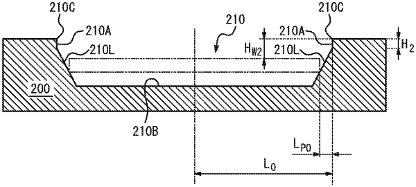
1. A susceptor for placing a silicon wafer thereon within an epitaxial growth apparatus,
the susceptor being provided with a concave counterbore portion in which the silicon wafer is placed,
wherein a difference between heights of an upper end and a lower end of an inner wall surface on the opening edge side of the counterbore portion varies at 90° periods in the circumferential direction, and when an angle at which the height difference is maximum is 0°, the height difference is maximum at 90°, 180°, and 270°, and the height difference is minimum at 45°, 135°, 225°, and 315°, and
in a projection view of a radial exterior of the susceptor, the opening edge of the counterbore portion describes four elliptical arcs being convex on the bottom side of the counterbore portion, wherein the silicon wafer is placed so that a <110> direction of the silicon wafer conforms to the direction of 0° of the susceptor, and in an epitaxial silicon wafer in which an epitaxial layer is formed on a surface of the silicon wafer, the elliptical arcs are provided such that a circumferential thickness profile variation index Δt0 of the epitaxial layer at a position of 1 mm from an edge of the epitaxial silicon wafer in a circumferential direction according to Equation 1 below is 0.75% or less,
 where tMax is a maximum thickness of the epitaxial layer at the position of 1 mm from the edge in the circumferential direction, tMin is a minimum thickness of the epitaxial layer at the position of 1 mm from the edge in the circumferential direction, and tAve is an average thickness of the epitaxial layer at the position of 1 mm from the edge in the circumferential direction.
|