| CPC H01L 21/6835 (2013.01) [H01L 21/288 (2013.01); H01L 21/31058 (2013.01); H01L 21/311 (2013.01); H01L 21/561 (2013.01); H01L 21/568 (2013.01); H01L 21/76834 (2013.01); H01L 21/76885 (2013.01); H01L 21/78 (2013.01); H01L 23/3128 (2013.01); H01L 23/3135 (2013.01); H01L 23/481 (2013.01); H01L 24/03 (2013.01); H01L 24/05 (2013.01); H01L 24/19 (2013.01); H01L 24/20 (2013.01); H01L 24/94 (2013.01); H01L 24/32 (2013.01); H01L 24/73 (2013.01); H01L 24/92 (2013.01); H01L 25/0657 (2013.01); H01L 2221/68359 (2013.01); H01L 2224/0231 (2013.01); H01L 2224/0237 (2013.01); H01L 2224/0391 (2013.01); H01L 2224/0401 (2013.01); H01L 2224/04042 (2013.01); H01L 2224/04105 (2013.01); H01L 2224/05124 (2013.01); H01L 2224/05147 (2013.01); H01L 2224/05166 (2013.01); H01L 2224/12105 (2013.01); H01L 2224/32145 (2013.01); H01L 2224/32225 (2013.01); H01L 2224/73265 (2013.01); H01L 2224/73267 (2013.01); H01L 2224/92244 (2013.01); H01L 2224/94 (2013.01); H01L 2224/97 (2013.01); H01L 2225/0651 (2013.01); H01L 2225/06568 (2013.01); H01L 2225/1035 (2013.01); H01L 2225/1058 (2013.01); H01L 2924/01029 (2013.01); H01L 2924/01047 (2013.01); H01L 2924/0105 (2013.01); H01L 2924/014 (2013.01); H01L 2924/05042 (2013.01); H01L 2924/05442 (2013.01); H01L 2924/1434 (2013.01); H01L 2924/1436 (2013.01); H01L 2924/1437 (2013.01); H01L 2924/351 (2013.01)] | 20 Claims |

|
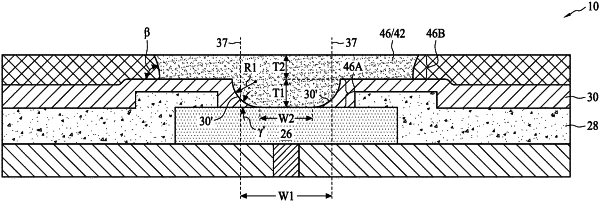
1. A package comprising:
a device die comprising:
a metal pad;
a first polymer layer covering edge portions of the metal pad; and
a metal pillar extending into the first polymer layer, wherein a first sidewall of the first polymer layer contacts a second sidewall of metal pillar to form a first interface;
an encapsulant encapsulating the device die therein;
a second polymer layer over the encapsulant and the device die; and
a redistribution line having a via portion extending into the second polymer layer, wherein the via portion comprises a third sidewall contacting a fourth sidewall of the second polymer layer to form a second interface, and wherein the first interface is more curved than the second interface.
|