| CPC H01L 21/3212 (2013.01) [H01L 21/30625 (2013.01); H01L 21/823431 (2013.01)] | 20 Claims |
|
1. A method of manufacturing a semiconductor device, comprising:
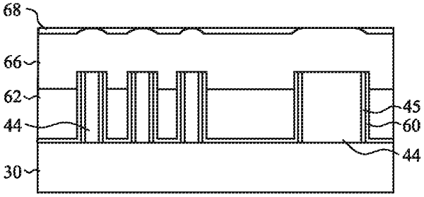
forming a sacrificial gate structure over a substrate, the sacrificial gate structure including a sacrificial gate electrode including a polysilicon or amorphous silicon layer;
forming a first dielectric layer over the sacrificial gate structure;
forming a second dielectric layer over the first dielectric layer;
planarizing and recessing the second and first dielectric layers such that an upper portion of the sacrificial gate structure is exposed and the polysilicon or amorphous silicon layer of the sacrificial gate electrode is exposed while a lower portion of the sacrificial gate structure is embedded in the first dielectric layer;
forming a third dielectric layer over the exposed sacrificial gate structure and over the first dielectric layer;
forming a fourth dielectric layer over the third dielectric layer;
planarizing the fourth and third dielectric layers such that the polysilicon or amorphous silicon layer of the sacrificial gate electrode is exposed and part of the third dielectric layer remains on the recessed first dielectric layer; and
removing the sacrificial gate electrode,
wherein the planarizing the fourth and third dielectric layers includes:
a first chemical mechanical polishing (CMP) process for etching the fourth dielectric layer;
a second CMP process for etching the third dielectric layer, which ends when the polysilicon or amorphous silicon layer of the sacrificial gate electrode is exposed; and
a third CMP process for recessing the third dielectric layer and the sacrificial gate electrode,
when the first CMP process is finished, a part of the fourth dielectric layer remains over the third dielectric layer.
|