| CPC H01J 37/32183 (2013.01) [H01J 37/32165 (2013.01); H01J 37/32568 (2013.01); H01L 21/31116 (2013.01); H01J 2237/334 (2013.01)] | 20 Claims |
|
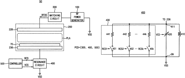
1. A plasma control device, comprising:
a matching circuit connected to a first electrode of a plasma chamber including the first electrode and a second electrode, the matching circuit configured to match impedance of a radio frequency (RF) power by an RF driving signal with an impedance of the first electrode, the RF driving signal being based on a first RF signal having a first frequency;
a resonance circuit connected between the second electrode and a ground voltage, the resonance circuit configured to control plasma distribution within the plasma chamber by providing resonance with respect to harmonics associated with the first frequency and by adjusting a ground impedance between the second electrode and the ground voltage; and
a controller configured to provide the resonance circuit with a capacitance control signal associated with the resonance and switch control signals associated with the ground impedance,
wherein the resonance circuit includes
a switching resistor circuit connected between a first node coupled to the second electrode and a ground node coupled to the ground voltage, the switching resistor circuit configured to adjust the ground impedance by providing different resistance values in response to the switch control signals, and
a variable capacitor connected between the first node and the ground node in parallel with the switching resistor circuit.
|