| CPC H01G 4/1227 (2013.01) [H01G 4/008 (2013.01); H01G 4/012 (2013.01); H01G 4/30 (2013.01)] | 8 Claims |
|
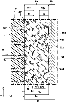
1. A ceramic electronic device comprising:
an element body including a ceramic layer and an internal electrode layer; and
an external electrode formed on an end surface of the element body and electrically connected to a part of the internal electrode layer, wherein
the ceramic layer comprises a perovskite compound represented by ABO3 as a main component,
the external electrode comprises a baked electrode layer,
the baked electrode layer comprises:
a first region contacted with the end surface of the element body and located near a joint boundary with the element body; and
a second region located outside the first region and constituting an outer surface of the baked electrode layer,
the first region comprises a glass frit including at least B and Si as a main component,
the second region comprises an Al based oxide mainly including Al and
an Al content of the Al based oxide is 0.3 parts by mol or more, provided that a total amount of elements other than oxygen contained in the Al based oxide is 1 part by mol.
|