| CPC H01G 4/1209 (2013.01) [H01G 4/30 (2013.01); H01G 4/012 (2013.01); H01G 4/232 (2013.01)] | 22 Claims |
|
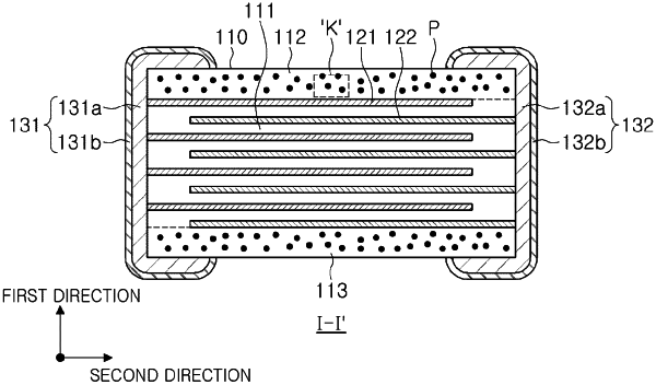
1. A multilayer electronic component comprising:
a body including a capacitance forming portion in which dielectric layers and internal electrodes are alternately disposed in a first direction, and cover portions disposed on an upper surface and a lower surface of the capacitance forming portion, respectively, in the first direction; and
external electrodes disposed on the body,
wherein the cover portion includes a plurality of dielectric grains and a plurality of pores, and
Gn/Pn is in a range from 12 to 29, in which Gn is number of dielectric grains included in the cover portion and Pn is number of pores included in the cover portion.
|