| CPC G11C 29/50004 (2013.01) [G01R 19/16528 (2013.01); G01R 19/16533 (2013.01); G11C 29/12005 (2013.01); G11C 2029/5004 (2013.01)] | 20 Claims |
|
1. A memory device comprising:
one or more memory banks;
a memory controller configured to provide instructions to determine whether voltage levels of one or more test signals associated with the one or more memory banks are within acceptable voltage ranges of the one or more memory banks; and
a voltage testing circuit comprising:
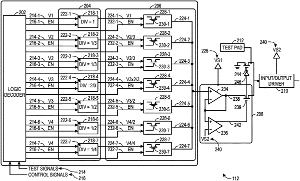
a divider circuit configured to:
receive the one or more test signals, wherein the one or more test signals have a voltage level above a high voltage threshold of the divider circuit; and
divide the one or more test signals by one or more division ratios associated with each of the one or more test signals based on the instructions, wherein dividing the one or more test signals comprises determining one or more divided test signals with voltage levels equal to or below the high voltage threshold; and
an amplification circuit comprising an amplifier, wherein the amplifier is configured to:
receive the one or more divided test signals;
receive a first supply voltage higher than the high voltage threshold providing a headroom voltage gap between the high voltage threshold and the first supply voltage; and
provide one or more amplified divided test signals based on receiving the one or more divided test signals to determine whether the voltage level of the one or more test signals are within the acceptable voltage ranges.
|