| CPC G11C 16/3459 (2013.01) [G11C 16/08 (2013.01); G11C 16/10 (2013.01); G11C 16/24 (2013.01); G11C 16/0483 (2013.01)] | 11 Claims |

|
1. A memory device comprising:
a plurality of memory cells coupled between a plurality of word lines and a plurality of bit lines;
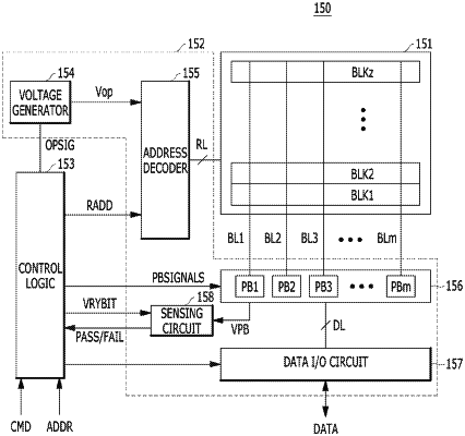
a control circuit suitable for performing a program loop including a program operation including a program voltage application operation on a selected word line among the plurality of word lines and a bit line setup operation on the plurality of bit lines and a verification operation of applying (N−1) first verification voltages to the selected word line according to a predetermined order to check N types of first program states for each of the plurality of memory cells included in the selected word line; and
control logic suitable for controlling the control circuit to repeatedly perform the program loop until programming for the selected word line is completed, and controlling the control circuit to apply any one of N types of column voltages to each of the plurality of bit lines in the bit line setup operation included in a second program loop according to a result of performing the verification operation included in a first program loop,
wherein the control circuit applies (N−1) second verification voltages to the selected word line according to the predetermined order to check N types of second program states for each of the plurality of memory cells included in the selected word line in the verification operation, and a maximum level of the second verification voltages is higher than a maximum level of the first verification voltages, and
wherein “N” is a natural number equal to or greater than 4.
|