| CPC G11C 16/32 (2013.01) [G11C 16/0483 (2013.01); H01L 25/0657 (2013.01); H01L 2225/06506 (2013.01)] | 20 Claims |
|
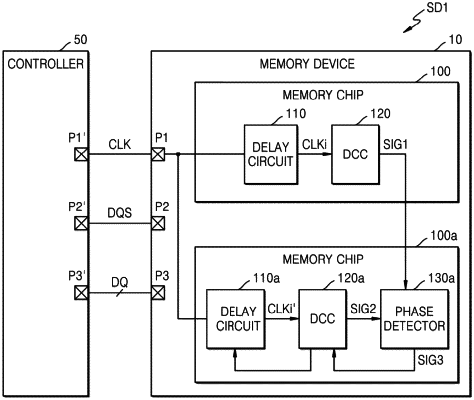
1. A nonvolatile memory device comprising:
a buffer chip configured to generate a first clock signal and a second clock signal from a clock signal received from a controller;
a first memory chip configured to generate a first signal from a first internal clock signal, which is based on the first clock signal; and
a second memory chip configured to generate a second signal from a second internal clock signal, which is based on the second clock signal,
wherein the buffer chip is configured to perform a phase calibration operation on the second signal based on a phase of the first signal by delaying the second clock signal based on a phase difference between the first and second signals,
wherein at least one of the first memory chip or the second memory chip is a vertical NAND flash memory chip, and
wherein the vertical NAND flash memory chip includes,
word lines stacked on a substrate in a vertical direction, and
cell strings each including a plurality of memory cells, which are connected to the word lines, respectively.
|