US 11,984,163 B2
Processing unit with fast read speed memory device
Deepak Chandra Sekar, San Jose, CA (US); Gary Bela Bronner, Los Altos, CA (US); and Frederick A. Ware, Los Altos Hills, CA (US)
Assigned to Hefei Reliance Memory Limited, Hefei (CN)
Filed by HEFEI RELIANCE MEMORY LIMITED, Hefei (CN)
Filed on Feb. 4, 2022, as Appl. No. 17/665,123.
Application 17/665,123 is a continuation in part of application No. 17/022,508, filed on Sep. 16, 2020, granted, now 11,257,544.
Application 17/022,508 is a continuation of application No. 16/521,126, filed on Jul. 24, 2019, granted, now 10,825,518, issued on Nov. 3, 2020.
Application 16/521,126 is a continuation of application No. 15/948,044, filed on Apr. 9, 2018, granted, now 10,388,375, issued on Aug. 20, 2019.
Application 15/948,044 is a continuation of application No. 15/338,872, filed on Oct. 31, 2016, granted, now 9,941,005, issued on Apr. 10, 2018.
Application 15/338,872 is a continuation of application No. 14/987,309, filed on Jan. 4, 2016, granted, now 9,490,009, issued on Nov. 8, 2016.
Application 14/987,309 is a continuation of application No. 14/210,085, filed on Mar. 13, 2014, granted, now 9,230,641, issued on Jan. 5, 2016.
Claims priority of provisional application 61/794,872, filed on Mar. 15, 2013.
Prior Publication US 2022/0157378 A1, May 19, 2022
This patent is subject to a terminal disclaimer.
Int. Cl. G11C 11/00 (2006.01); G11C 13/00 (2006.01)
CPC G11C 13/0069 (2013.01) [G11C 13/0002 (2013.01); G11C 13/0007 (2013.01); G11C 13/0023 (2013.01); G11C 13/003 (2013.01); G11C 13/004 (2013.01); G11C 13/0097 (2013.01); G11C 2213/15 (2013.01); G11C 2213/72 (2013.01); G11C 2213/74 (2013.01); G11C 2213/75 (2013.01); G11C 2213/78 (2013.01); G11C 2213/79 (2013.01)] 20 Claims
OG exemplary drawing
 
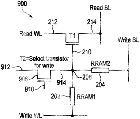
1. A graphics processing unit (GPU) comprising:
a plurality of memory cells, each of the memory cells comprising:
a first memory comprising a first terminal electrically coupled with a common node and a second terminal electrically coupled with a write word line;
a second memory comprising a third terminal electrically coupled with the first memory at the common node and a fourth terminal electrically coupled with a write bit line; and
a first switch comprising a fifth terminal and a sixth terminal, wherein the fifth terminal is electrically coupled with the common node and a control terminal and the sixth terminal is electrically coupled to a word line.