| CPC G11C 13/0059 (2013.01) [G11C 13/0004 (2013.01); G11C 13/003 (2013.01); H10B 63/24 (2023.02); H10B 63/80 (2023.02); H10N 70/063 (2023.02); H10N 70/231 (2023.02); H10N 70/882 (2023.02); G11C 2213/72 (2013.01)] | 15 Claims |
|
1. An apparatus comprising:
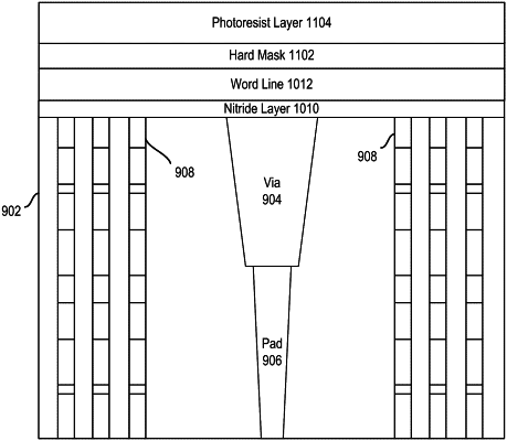
a memory array comprising memory cells;
an access line configured to access the memory cells, the access line having a first conductive portion and a second conductive portion on opposite sides of the access line;
a first insulating layer in an interior region of the access line, the first insulating layer underlying or overlying a first memory cell; and
a second insulating layer in the interior region of the access line and parallel to the first insulating layer, wherein the second insulating layer is vertically above or below the first insulating layer;
wherein a lateral length of the first insulating layer is different than a lateral length of the second insulating layer;
wherein memory cells above the access line have a type or structure different from memory cells below the access line;
the first insulating layer has a structure corresponding to the memory cells below the access line; and
the second insulating layer has a structure corresponding to the memory cells above the access line.
|