| CPC G11C 11/4085 (2013.01) [H01L 27/1207 (2013.01); H01L 27/1225 (2013.01); H01L 27/124 (2013.01); H01L 27/1255 (2013.01); H01L 29/24 (2013.01); H01L 29/78648 (2013.01); H01L 29/7869 (2013.01); H10B 99/00 (2023.02)] | 4 Claims |
|
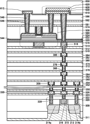
1. A semiconductor device comprising a transistor, the semiconductor device comprising:
a first conductive film comprising a region being a first gate electrode of the transistor;
a first insulating film over the first conductive film;
an oxide semiconductor film over the first insulating film;
a second insulating film over the oxide semiconductor film;
a second conductive film comprising a region being a second gate electrode of the transistor, over the second insulating film;
a third insulating film over the second conductive film;
a third conductive film in contact with an upper surface of the third insulating film;
a fourth conductive film in contact with the upper surface of the third insulating film; and
a fifth conductive film in contact with the upper surface of the third insulating film,
wherein the oxide semiconductor film comprises a channel formation region of the transistor,
wherein the third conductive film is electrically connected to the oxide semiconductor film,
wherein the fourth conductive film is electrically connected to the first conductive film,
wherein the fifth conductive film is electrically connected to the second conductive film,
wherein the fourth conductive film comprises a region extending along a first direction, and
wherein the fifth conductive film comprises a region extending along the first direction.
|