| CPC G11C 11/4085 (2013.01) [G11C 11/4074 (2013.01); G11C 11/4094 (2013.01); G11C 11/4096 (2013.01)] | 32 Claims |
|
1. A circuit, comprising:
a memory array including a plurality of static random access memory (SRAM) cells arranged in a matrix with plural rows and plural columns, each row including a word line connected to the SRAM cells of the row, and each column including at least one bit line connected to the SRAM cells of the column;
a word line driver circuit for each row having an output connected to drive the word line of the row;
a row controller circuit configured to simultaneously actuate the plurality of word lines by applying pulses through the word line driver circuits to the word lines for an in-memory compute operation;
a column processing circuit connected to the at least one bit line for each column and configured to process analog voltages developed on the bit lines in response to the simultaneous actuation of the plurality of word lines to generate a decision output for the in-memory compute operation; and
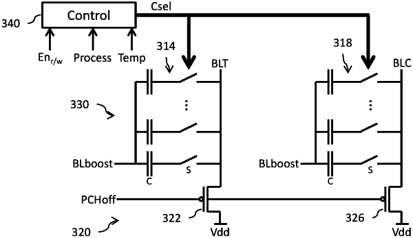
a bit line precharge circuit configured to generate a precharge voltage for application to the at least one bit line for each column, wherein the precharge voltage has a first voltage level not greater than a positive supply voltage for the plurality of SRAM cells when the memory array is operating in a data read/write mode, and wherein the precharge voltage has a second voltage level greater than the first voltage level in advance of the simultaneous actuation of the plurality of word lines for the in-memory compute operation.
|