| CPC G11C 11/4085 (2013.01) [G11C 11/221 (2013.01); G11C 11/2257 (2013.01); G11C 11/2259 (2013.01); G11C 11/4087 (2013.01); H01L 24/08 (2013.01); H01L 24/80 (2013.01); H01L 25/0657 (2013.01); H01L 25/18 (2013.01); H01L 25/50 (2013.01); H01L 2224/08145 (2013.01); H01L 2224/80895 (2013.01); H01L 2224/80896 (2013.01); H01L 2924/1431 (2013.01); H01L 2924/1436 (2013.01); H01L 2924/1441 (2013.01)] | 25 Claims |
|
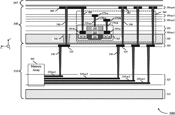
1. An apparatus comprising:
a first semiconductor die comprising a plurality of word line conductors arranged in a stack along a first direction away from a substrate of the first semiconductor die, each word line conductor of the plurality of word line conductors extending along a second direction over the substrate and operable to access a respective set of one or more memory cells of the first semiconductor die;
a second semiconductor die comprising a plurality of word line driver circuits, each word line driver circuit of the plurality of word line driver circuits operable to bias a respective word line conductor of the plurality of word line conductors based at least in part on a first word line decoder signal and a respective second word line decoder signal of a plurality of second word line decoder signals; and
a plurality of electrical contacts, each electrical contact of the plurality of electrical contacts coupling a respective word line conductor of the plurality of word line conductors with a respective word line driver circuit of the plurality of word line driver circuits.
|