| CPC G09G 3/3677 (2013.01) [G09G 3/3674 (2013.01); G11C 19/00 (2013.01); H01L 27/0207 (2013.01); H01L 27/1214 (2013.01); H01L 27/1225 (2013.01); H01L 27/124 (2013.01); H01L 29/7869 (2013.01); H03K 17/687 (2013.01); H03K 19/0013 (2013.01); H03K 19/018557 (2013.01); H03K 19/018571 (2013.01); G09G 2310/0251 (2013.01); G09G 2310/0286 (2013.01); G09G 2310/0289 (2013.01); G09G 2310/08 (2013.01); G09G 2330/021 (2013.01)] | 13 Claims |
|
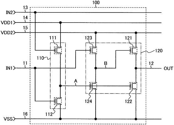
1. A liquid crystal display device comprising:
a first scan line driver circuit configured to drive a first gate signal line;
a second scan line driver circuit configured to drive a second gate signal line; and
a pixel portion between the first scan line driver circuit and the second scan line driver circuit, the pixel portion comprising a pixel,
wherein at least one of the first scan line driver circuit and the second scan line driver circuit comprises a first transistor, a second transistor, a third transistor, a fourth transistor, a fifth transistor, a sixth transistor, and a seventh transistor,
wherein one of a source and a drain of the first transistor is electrically connected to one of a source and a drain of the second transistor, one of a source and a drain of the seventh transistor, and a first wiring,
wherein one of a source and a drain of the third transistor is electrically connected to one of a source and a drain of the fourth transistor,
wherein one of a source and a drain of the fifth transistor is electrically connected to one of a source and a drain of the sixth transistor,
wherein the other of the source and the drain of the first transistor is electrically connected to a second wiring,
wherein a gate of the first transistor is electrically connected to the one of the source and the drain of the third transistor and the one of the source and the drain of the fourth transistor,
wherein the other of the source and the drain of the second transistor is electrically connected to the other of the source and the drain of the seventh transistor and a third wiring,
wherein the other of the source and the drain of the fourth transistor is electrically connected to the other of the source and the drain of the sixth transistor,
wherein a gate of the second transistor is electrically connected to a gate of the fourth transistor, the one of the source and the drain of the fifth transistor, and the one of the source and the drain of the sixth transistor,
wherein the other of the source and the drain of the fifth transistor is electrically connected to a fifth wiring,
wherein a gate of the fifth transistor is electrically connected to a sixth wiring,
wherein a gate of the seventh transistor is electrically connected to a seventh wiring,
wherein the second wiring is configured to supply a first clock signal,
wherein the third wiring is configured to supply a first power supply voltage,
wherein the fifth wiring is configured to supply a second power supply voltage which is higher than the first power supply voltage, and
wherein the sixth wiring is configured to supply a second clock signal.
|