| CPC G09G 3/3266 (2013.01) [G09G 3/3275 (2013.01); G09G 2300/0809 (2013.01); G09G 2320/0209 (2013.01); G09G 2320/0233 (2013.01); G09G 2330/021 (2013.01)] | 19 Claims |
|
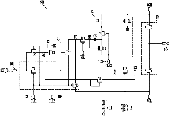
1. A gate driver comprising a stage configured to output a gate signal, the stage comprising:
a first input terminal configured to receive an output signal of a previous stage or a start pulse;
a second input terminal configured to receive a first clock signal;
a third input terminal configured to receive a second clock signal that is shifted from the first clock signal;
a first power source;
a second power source;
an input part comprising a fourth transistor and configured to control a voltage of a first node and a voltage of a second node based on signals supplied to the first input terminal and the second input terminal, wherein the fourth transistor is connected between the first input terminal and the first node and comprises a gate electrode connected to the second input terminal;
an output part comprising a seventh transistor and an eighth transistor and configured to supply a voltage of the first power source or a voltage of the second power source as the gate signal to an output terminal based on a voltage of a third node and a voltage of a fourth node, wherein the seventh transistor is connected between the first power source and the output terminal and comprises a gate electrode connected to the third node, and wherein the eighth transistor is connected between the second power source and the output terminal and comprises a gate electrode connected to the fourth node;
a first signal processing part comprising an eleventh transistor and configured to supply the voltage of the second power source to the fourth node based on the voltage of the first node, or to electrically connect the second node and the fourth node through a fifth node based on a signal supplied to the third input terminal, wherein the eleventh transistor is connected between the second power source and the fourth node and comprises a gate electrode connected to the first node; and
a second signal processing part comprising a first transistor that is diode-connected between the third node and a sixth node, and that comprises a gate electrode coupled to the sixth node, to control the voltage of the third node based on an operation of the first transistor.
|