| CPC G09G 3/3233 (2013.01) [H10K 59/131 (2023.02); G09G 2300/0408 (2013.01); G09G 2300/0819 (2013.01); G09G 2300/0842 (2013.01); G09G 2300/0861 (2013.01); G09G 2320/0233 (2013.01)] | 20 Claims |

|
1. A display panel, comprising:
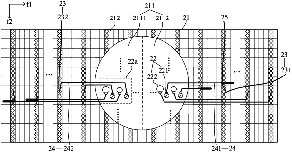
a substrate, comprising a light-transmissive display region and a conventional display region surrounding the light-transmissive display region;
a plurality of light-emitting elements disposed in the light-transmissive display region, a plurality of pixel drive circuits disposed in the conventional display region, and a plurality of connection lines and a plurality of compensation portions that are disposed on the substrate; wherein
the plurality of light-emitting elements are arranged along a first direction; and
the plurality of pixel drive circuits are electrically connected to the plurality of light-emitting elements and at least comprise a first pixel drive circuit and a second pixel drive circuit, wherein the first pixel drive circuit and the second pixel drive circuit are respectively disposed on two sides of the light-transmissive display region in the first direction and are respectively electrically connected to the plurality of light-emitting elements by the connection lines, the connection lines comprising a first connection line and a second connection line, a length of the first connection line electrically connected to the first pixel drive circuit being less than a length of the second connection line electrically connected to the second pixel drive circuit, the compensation portion being electrically connected to the first connection line, and the first connection line and the second connection line being two connection lines in the plurality of connection lines.
|