| CPC G09G 3/3233 (2013.01) [G09G 3/3266 (2013.01); G09G 3/3291 (2013.01); G09G 2300/0819 (2013.01); G09G 2300/0842 (2013.01); G09G 2300/0852 (2013.01); G09G 2300/0861 (2013.01); G09G 2310/0243 (2013.01); G09G 2310/08 (2013.01); G09G 2320/0233 (2013.01); G09G 2320/0238 (2013.01); G09G 2330/028 (2013.01)] | 20 Claims |
|
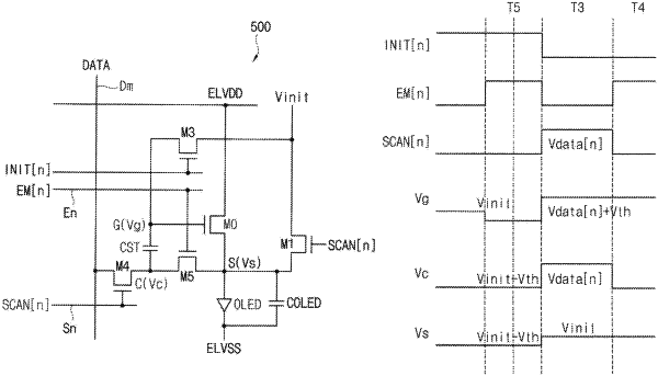
1. A pixel circuit comprising:
a light emission element;
a driving transistor including a first electrode electrically connected to the light emission element, a second electrode, and a gate electrode;
a first transistor including a first electrode, a second electrode, and a gate electrode which receives a fourth signal, one of the first electrode and the second electrode of the first transistor electrically connected to the first electrode of the driving transistor;
a second transistor including a first electrode electrically connected to a line transferring a power voltage, a second electrode electrically connected to the second electrode of the driving transistor, and a gate electrode which receives a first signal;
a third transistor including a first electrode electrically connected to the second electrode of the driving transistor, a second electrode electrically connected to the gate electrode of the driving transistor, and a gate electrode which receives a second signal;
a storage capacitor including a first electrode and a second electrode, one of the first electrode and the second electrode of the storage capacitor electrically connected to the gate electrode of the driving transistor; and
a switching transistor including a first electrode, a second electrode, and a gate electrode which receives a third signal, one of the first electrode and the second electrode of the switching transistor electrically connected to a data line.
|