| CPC G09G 3/32 (2013.01) [H10K 59/131 (2023.02); G09G 2300/0819 (2013.01); G09G 2300/0842 (2013.01); G09G 2310/02 (2013.01); G09G 2310/08 (2013.01); G09G 2330/021 (2013.01)] | 15 Claims |
|
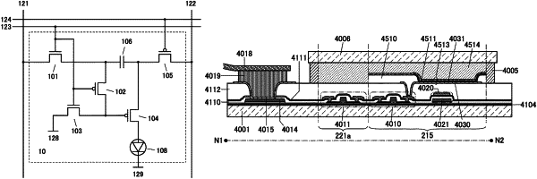
1. A display apparatus comprising a pixel, the pixel comprising:
a first transistor;
a second transistor;
a third transistor;
a fourth transistor;
a fifth transistor;
a capacitor; and
a light-emitting device,
wherein one of a source and a drain of the first transistor is electrically connected to one of a source and a drain of the second transistor and one electrode of the capacitor,
wherein the other of the source and the drain of the second transistor is electrically connected to one of a source and a drain of the third transistor and a gate of the fourth transistor,
wherein one of a source and a drain of the fourth transistor is electrically connected to the other electrode of the capacitor and one of a source and a drain of the fifth transistor,
wherein the other of the source and the drain of the fourth transistor is electrically connected to the light-emitting device,
wherein a gate of the first transistor and a gate of the third transistor are electrically connected to a first gate line,
wherein a gate of the fifth transistor is electrically connected to a second gate line,
wherein each of the first transistor and the third transistor is an n-channel transistor,
wherein the fourth transistor is a p-channel transistor,
wherein each of the first transistor and the third transistor comprises a first material in a channel formation region,
wherein the fourth transistor comprises a second material in a channel formation region, and
wherein the first material is different from the second material.
|