| CPC G09G 3/32 (2013.01) [G09G 2300/0819 (2013.01); G09G 2300/0852 (2013.01); G09G 2310/0278 (2013.01); G09G 2320/0233 (2013.01); G09G 2320/045 (2013.01)] | 30 Claims |
|
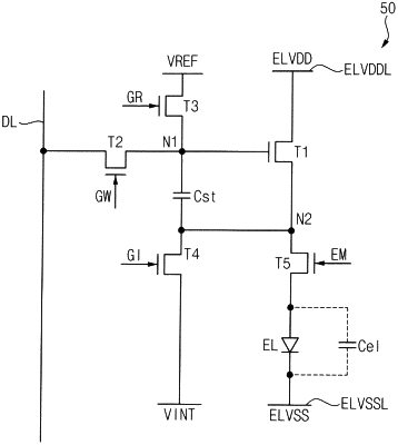
1. A pixel of a display device, the pixel comprising:
a first transistor including a gate coupled to a first node, a first terminal coupled to a first power supply voltage line, and a second terminal coupled to a second node;
a first capacitor coupled between the first node and the second node;
a second transistor including a gate, which receives a first signal, a first terminal coupled to a data line, and a second terminal coupled to the first node;
a third transistor including a gate, which receives a second signal, a first terminal, which receives a reference voltage, and a second terminal coupled to the first node;
a fourth transistor including a gate, which receives a third signal, a first terminal coupled to the second node, and a second terminal, which receives an initialization voltage;
a light emitting element including an anode, and a cathode coupled to a second power supply voltage line; and
a fifth transistor including a gate, which receives a fourth signal, a first terminal coupled to the second node, and a second terminal coupled to the anode,
wherein each frame period for the pixel includes a threshold voltage compensation period in which a threshold voltage of the first transistor is stored in the first capacitor,
wherein, in the threshold voltage compensation period, the second signal has an active level, the first signal, the third signal and the fourth signal have an inactive level, the third transistor is turned on in response to the second signal having the active level to apply the reference voltage to the first node, the first transistor operates as a source follower to change a voltage of the second node to a voltage corresponding to the threshold voltage of the first transistor subtracted from the reference voltage, and the fifth transistor is turned off in response to the fourth signal having the inactive level to separated the second node from anode.
|