| CPC G09G 3/2092 (2013.01) [G09G 3/3266 (2013.01); G09G 2310/0267 (2013.01); G09G 2310/08 (2013.01); G09G 2320/0219 (2013.01); G09G 2330/021 (2013.01)] | 20 Claims |
|
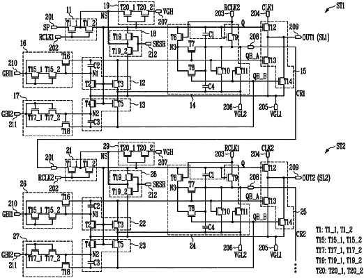
1. A scan driver, the scan driver comprising stages, the stages including a first stage, the scan driver comprising:
a plurality of stages that supply scan signals to scan lines based on a first clock signal, a first carry clock signal, a second carry clock signal, a first power source voltage, and a second power source voltage,
wherein the first stage includes:
a first power input terminal receiving the first power source voltage;
a second power input terminal receiving the second power source voltage;
a first input terminal receiving an input signal;
a second input terminal receiving the first carry clock signal;
a third input terminal receiving the second carry clock signal;
a fourth input terminal receiving the first clock signal;
a first node;
an input circuit controlling a voltage of the first node based on the input signal and the first carry clock signal;
a first control circuit controlling a voltage of a second node based on the first power source voltage, the second power source voltage, and the voltage of the first node, wherein the second node is included in at least one of the first control circuit and the first stage;
a second control circuit controlling a voltage of a third node based on the first power source voltage, the second power source voltage, and the voltage of the first node, wherein the third node is included in at least one of the second control circuit and the first stage;
a first output terminal;
a first output circuit outputting a first carry signal through the first output terminal based on the voltage of the first node, the voltage of the second node, the voltage of the third node, the second power source voltage, and the second carry clock signal;
a second output terminal; and
a second output circuit outputting a first scan signal through the second output terminal based on the voltage of the first node, the voltage of the second node, the voltage of the third node, the first power source voltage, and the first clock signal, and
wherein, throughout at least a portion of one frame, each of the first clock signal, the first carry clock signal, and the second carry clock signal is constant.
|