| CPC G09G 3/006 (2013.01) [G01R 31/2635 (2013.01); G09G 3/32 (2013.01); G09G 2330/10 (2013.01); G09G 2330/12 (2013.01); H10K 59/12 (2023.02)] | 9 Claims |
|
1. A display device including a plurality of pixels each including at least one light-emitting element, the display device including
an inspection circuit configured to inspect a luminance condition of the at least one light-emitting element, the inspection circuit comprising:
a voltage sweep circuit configured to sweep a voltage to the at least one light-emitting element;
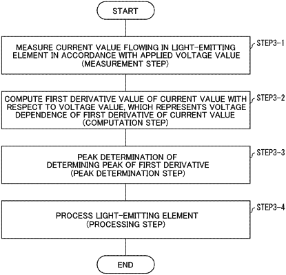
a measuring circuit configured to sweep a voltage to the at least one light-emitting element and to measure a current value that flows in the at least one light-emitting element in response to a voltage value applied;
a computation circuit configured to compute a first derivative value of the current value with respect to the voltage value, the first derivative value representing voltage dependence of a first derivative of the current value;
a peak determination circuit configured to determine whether the first derivative value has a local maximum value; and
a processing circuit configured to blacken the at least one light-emitting element based on a result of the determination made by the peak determination circuit.
|