| CPC G09F 9/30 (2013.01) [G06F 3/0412 (2013.01); H01L 25/0753 (2013.01); H01L 33/58 (2013.01)] | 20 Claims |
|
1. A product comprising;
a transparent conductive sheet;
a display panel;
a thin layer that covers at least a portion of a front surface of the display panel; and
a transparent substrate that forms a light guiding path, the light guiding path disposed in at least one of the following locations: at an opening between the transparent conductive sheet and the thin layer, or at an opening between the transparent conductive sheet and a light emitting device array substrate;
wherein the thin layer comprises at least one of the following: a nature derived wood, a natural fiber, a natural leather, a natural stone, or a material which imitates a natural appearance and a natural texture;
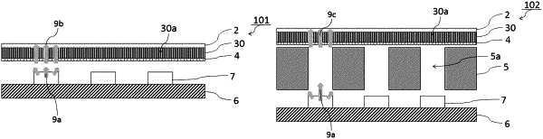
wherein the transparent substrate has micropores provided in a resin base material made of a transparent resin, said micropores are formed by a set of lattice-like louvers, and a gap between the lattice-like louvers provides a light waveguide along an optical axis of light emitting elements of the light emitting device array substrate; and
wherein the transparent substrate increases an amount of light reaching the thin layer, and a diffusion which occurs due to the thin layer widens a viewing angle of the display panel front surface and improves a visibility of the display panel when the display panel is emitting light.
|