| CPC G06T 7/001 (2013.01) [G03F 7/70666 (2013.01); G06T 1/0014 (2013.01); G01N 2021/8854 (2013.01); G06T 2207/10032 (2013.01); G06T 2207/30141 (2013.01); G06T 2207/30148 (2013.01)] | 20 Claims |
|
1. A mask inspection system, the system comprising:
an inspection tool configured to:
detect a runtime defect at a defect location on a mask of a semiconductor specimen during runtime scan of the mask; and
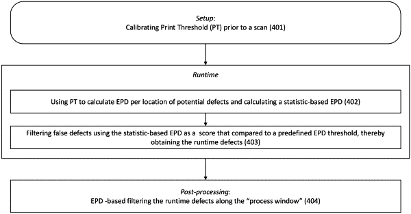
acquire, based on the defect location after runtime, a plurality of sets of aerial images of the runtime defect corresponding to a plurality of focus states throughout a focus process window, each set of aerial images acquired at a respective focus state; and
a processing and memory circuitry (PMC) operatively connected to the inspection tool and configured to:
for each set of aerial images, calculate a statistic-based Edge Positioning Displacement (EPD) value of the runtime defect, thereby giving rise to a plurality of statistic-based EPD values each corresponding to a respective focus state; and
determine whether the runtime defect is a true defect based on the plurality of statistic-based EPD values.
|