| CPC G06T 1/60 (2013.01) [G02B 27/017 (2013.01); H10K 59/131 (2023.02); G02B 2027/0112 (2013.01); G02B 2027/0118 (2013.01); G02B 2027/0123 (2013.01); G02B 2027/014 (2013.01); G02B 27/0172 (2013.01); G02B 2027/0178 (2013.01); H10K 59/35 (2023.02); H10K 59/38 (2023.02)] | 12 Claims |
|
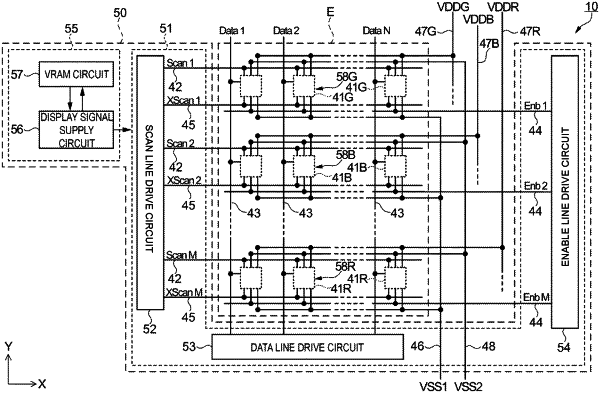
1. An electro-optical device comprising:
a first data line;
a second data line;
a scan line;
a first pixel circuit being provided in correspondence with an intersection of the first data line and the scan line, the first pixel circuit including a first light-emitting element, a first enable transistor and a first drive transistor;
a second pixel circuit being provided in correspondence with an intersection of the second data line and the scan line, the second pixel circuit including a second light-emitting element, a second enable transistor and a second drive transistor;
a first potential line supplying a first potential to the first pixel circuit;
a second potential line supplying a second potential to the second pixel circuit;
a third potential line supplying a third potential to the first pixel circuit and the second pixel circuit; and
a fourth potential line supplying a fourth potential to the first pixel circuit and the second pixel circuit, wherein
the first light-emitting element, the first enable transistor and the first drive transistor are disposed in series between the first potential line and the fourth potential line,
the second light-emitting element, the second enable transistor and the second drive transistor are disposed in series between the second potential line and the fourth potential line, and
the first enable transistor and the second enable transistor turn ON simultaneously.
|