| CPC G06F 3/0659 (2013.01) [G06F 3/0607 (2013.01); G06F 3/0679 (2013.01)] | 20 Claims |

|
1. An apparatus, comprising:
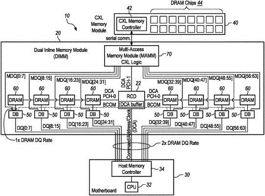
a plurality of data buffer and multiplexer devices, each data buffer and multiplexer device having host data contacts for communicating data signals with a host memory controller, first memory-side data contacts for communicating data signals with one of a plurality of dynamic random-access memory chips on a first memory module, second memory-side data contacts and a control line contact;
a registered clock driver having a host command and address contact for communicating command and address signals with the host memory controller, a first memory-side command and address contact for communicating command and address signals with the dynamic random-access memory chips of the first memory module, a second memory-side command and address contact, and a buffer communication contact connected to the control line; and
a data conversion module connected to the second memory-side data contacts for communicating data signals with the data buffer and multiplexer devices and connected to the second memory-side command and address contact for communicating command and address signals with the registered clock driver, the data conversion module for converting parallel data signals from the data buffer and multiplexer devices to serial data signals for communicating over a serial computer expansion bus with a second memory module and for converting serial data signals received from the second memory module over the serial computer expansion bus to parallel data signals for communicating with the data buffer and multiplexer devices;
wherein the data buffer and multiplexer devices communicate data signals with the host memory controller at twice the clock rate that the data buffer and multiplexer devices communicate data signals with the dynamic random-access memory chips and the data conversion module.
|