| CPC G06F 3/0412 (2013.01) [G02B 5/3025 (2013.01); G06F 3/047 (2013.01); H10K 50/805 (2023.02); H10K 50/84 (2023.02); H10K 59/122 (2023.02); H10K 59/124 (2023.02); H10K 59/131 (2023.02); H10K 59/38 (2023.02); H10K 71/00 (2023.02); H10K 77/111 (2023.02); H10K 59/40 (2023.02)] | 20 Claims |
|
1. An organic light emitting display (MED) device comprising:
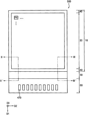
a substrate having a display region including a pixel region and a first peripheral region surrounding the pixel region, a second peripheral region that is spaced apart from the display region, and a bending region that is interposed between the display region and the second peripheral region;
a buffer layer disposed on the substrate, the buffer layer having a first removed region exposing a portion of an upper surface of the substrate, the first removed region overlapping, the bending region, a portion of the first peripheral region, and a portion of the second peripheral region;
a plurality of pixel structures disposed in the pixel region on the buffer layer;
an insulation layer structure including a plurality of insulation layers disposed on the buffer layer, the insulation layer structure having a second removed region exposing the first removed region and a top surface of a portion of the buffer layer that is disposed adjacent to the first removed region, the top surface being a surface of the buffer layer that faces away from, and is farthest from, the substrate;
a fan-out wiring disposed in the insulation layer structure, the fan-out wiring including a first fan-out wiring disposed in the first peripheral region and a second fan-out wiring disposed in the second peripheral region;
a first planarization layer disposed in the first peripheral region disposed adjacent to the bending region, the bending region, and the second peripheral region disposed adjacent to the bending region on the substrate; and
a connection electrode disposed on the first planarization layer, the connection electrode being electrically connected to the fan-out wiring.
|