| CPC G06F 3/0412 (2013.01) [G02F 1/13338 (2013.01); G06F 1/3265 (2013.01); G06F 3/044 (2013.01); G06F 3/045 (2013.01); G09G 3/3648 (2013.01); G09G 3/3677 (2013.01); G09G 3/3688 (2013.01); G09G 2300/0426 (2013.01); G09G 2310/0286 (2013.01); G09G 2310/08 (2013.01); G09G 2330/021 (2013.01); G09G 2360/14 (2013.01); Y02D 10/00 (2018.01)] | 7 Claims |
|
1. A display device comprising:
a pixel portion comprising a pixel;
a driver circuit configured to drive the pixel portion; and
a touch panel overlapping with the pixel portion,
wherein a supply of a start signal to the driver circuit is stopped,
wherein, after the supply of the start signal is stopped, a supply of a clock signal to the driver circuit is stopped,
wherein, after the supply of the clock signal is stopped, a power supply potential of the driver circuit is changed from a first potential into a second potential having a lower potential than the first potential,
wherein the pixel comprises a transistor comprising an oxide semiconductor film in a channel formation region,
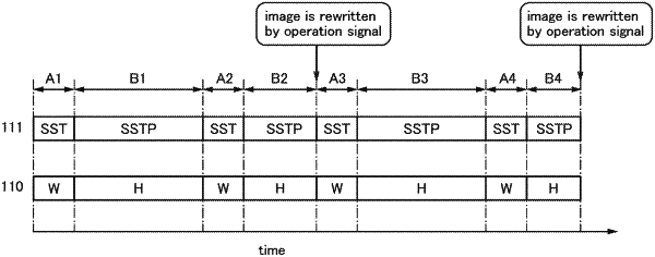
wherein a period in which a still image is displayed comprises:
a first period in which a state of the pixel is set; and
a second period in which the state of the pixel is held,
wherein a driving frequency of the driver circuit in the second period is lower than a driving frequency of the driver circuit in the first period, and
wherein the second period is terminated by an operation signal supplied from the touch panel.
|