| CPC G06F 13/20 (2013.01) [G06N 10/40 (2022.01); H01L 29/423 (2013.01); H01L 29/42316 (2013.01); H01L 29/66977 (2013.01); H03K 17/92 (2013.01); H10N 60/11 (2023.02); H10N 60/128 (2023.02); H10N 69/00 (2023.02); G06F 2213/40 (2013.01)] | 13 Claims |
|
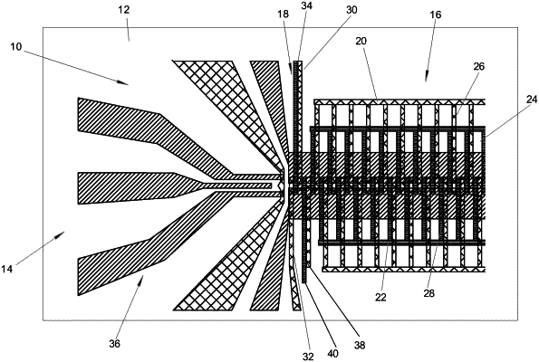
1. An electronic component, which is formed by a semiconductor component having gate electrode assemblies, for reading out a quantum state of a qubit in a quantum dot, comprising:
a substrate with a two-dimensional electron gas or electron hole gas;
electrical contacts for connecting the gate electrode assemblies to voltage sources;
gate electrode assemblies having gate electrodes, which are arranged on a surface of the electronic component, for producing potential wells in the substrate;
parallel electrode fingers being part of the gate electrodes of the gate electrode assemblies,
wherein in a first gate electrode assembly, the electrode fingers are interconnected in a periodically alternating manner, which causes an almost continuous movement of the potential well through the substrate, whereby a first quantum dot is transported together with this potential well, and
wherein the electrode fingers of a second gate electrode assembly form a static potential well in which a second charge carrier with a known quantum mechanical state is provided; and
a sensor element for detecting changes in the charge, which detects the charge in the static potential well, wherein the first quantum dot is transported to a second quantum dot.
|