| CPC G05B 13/042 (2013.01) [G05B 13/027 (2013.01); G06N 3/045 (2023.01); H01L 27/0207 (2013.01)] | 18 Claims |
|
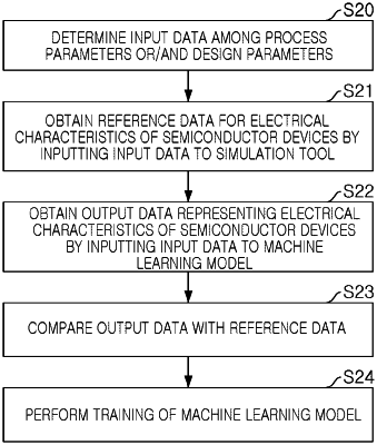
1. A simulation method for a semiconductor fabrication process, comprising:
obtaining, as input data, process parameters for controlling a semiconductor process of manufacturing semiconductor devices and design parameters representing a structure of the semiconductor devices;
generating predictive data for electrical characteristics of the semiconductor devices using a machine learning model based on the input data;
generating reference data for the electrical characteristics of the semiconductor devices using a simulation tool based on the input data;
training the machine learning model using the predictive data and the reference data, wherein the machine learning model comprises a first machine learning model configured to receive the process parameters and to output the design parameters representing a structure of the semiconductor devices, and a second machine learning model configured to receive the design parameters and to output the predictive data;
performing the semiconductor fabrication process using the output of the first machine learning model and the output of the second machine learning model.
|