| CPC G02F 1/1368 (2013.01) [G02F 1/134309 (2013.01); G02F 1/13629 (2021.01); G03B 21/006 (2013.01); G02F 1/133345 (2013.01); G02F 1/133526 (2013.01); G02F 1/136227 (2013.01)] | 14 Claims |
|
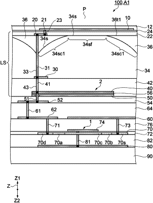
1. An electro-optical device, comprising:
a transistor;
a pixel electrode provided corresponding to the transistor;
a lens layer provided at a layer between the transistor and the pixel electrode;
a first light transmitting layer provided at a layer between the lens layer and the pixel electrode, and planarized together with the lens layer;
a first conductive layer provided at a layer between the transistor and the lens layer; and
a second conductive layer provided at a layer between the first light transmitting layer and the pixel electrode, and electrically connected to the first conductive layer via a first contact hole.
|