| CPC G02F 1/136286 (2013.01) [G02F 1/134318 (2021.01); G02F 1/13454 (2013.01); G02F 1/136222 (2021.01)] | 16 Claims |
|
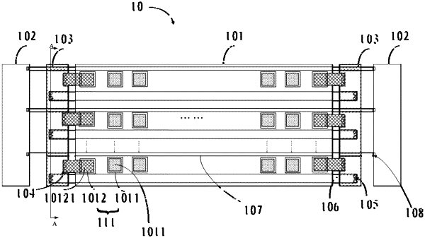
1. A liquid crystal display (LCD) panel, comprising a display area, a gate driver on array (GOA) circuit area, and a first common electrode line disposed between the display area and the GOA circuit area;
wherein a plurality of virtual pixels are disposed on a side of the display area near the GOA circuit area and are arranged along a column direction, each of the virtual pixels comprises a virtual pixel electrode, and the first common electrode line is connected to each of the virtual pixel electrodes,
wherein a plurality of display pixels used to display are disposed on the display area, and each of the display pixels comprises a display pixel electrode,
wherein the display pixel electrode has a strip-shaped vertical trunk, a strip-shaped horizontal trunk, and two strip-shaped branches having predetermined angles with respect to the horizontal trunk and the vertical trunk, and the virtual pixel electrodes are block-shaped.
|