| CPC G02F 1/1339 (2013.01) [G02F 1/133308 (2013.01); G02F 2202/28 (2013.01)] | 10 Claims |
|
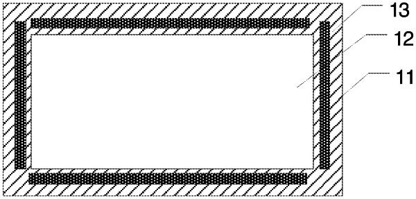
1. A display device, comprising:
a substrate;
a display panel comprising a display region and a non-display region surrounding the display region; and
a frame sealant layer configured to adhere the display panel and the substrate, wherein the fame sealant layer is correspondingly distributed in the non-display region of the display panel and surrounding the display region, the frame sealant layer comprises liquid adhesive regions and solid adhesive regions disposed at intervals, each of the liquid adhesive regions is provided with a liquid adhesive, and each of the solid adhesive regions is provided with a solid adhesive.
|