| CPC G02F 1/133603 (2013.01) [G02F 1/133605 (2013.01); G02F 1/133608 (2013.01); G02F 1/133612 (2021.01); G02F 1/133528 (2013.01); G02F 1/133607 (2021.01)] | 10 Claims |

|
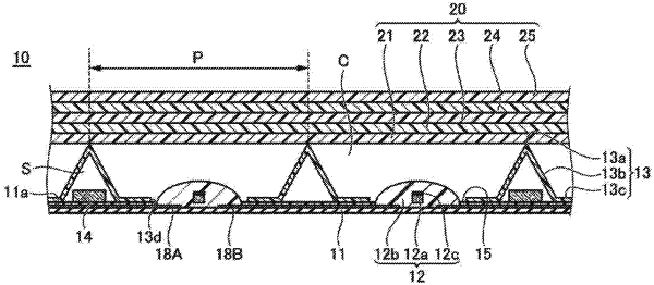
1. A light-emitting device comprising:
a plurality of light sources;
a board on which conductive wires supplying power to the plurality of light sources are disposed;
a cover member covering portions of the conductive wires that do not serve as electrical contacts;
a sectioning member including a wall part having a plurality of portions each surrounding one or more of the plurality of light sources in top view; and
one or more integrated circuits configured to drive the light sources,
wherein the sectioning member and the one or more integrated circuits are disposed on a same side of the board on which the light sources are disposed,
wherein a space is formed between a back surface of the sectioning member and the cover member on the board, and
wherein the one or more integrated circuits are disposed in the space.
|