| CPC G02B 6/4227 (2013.01) [G02B 6/4222 (2013.01)] | 18 Claims |

|
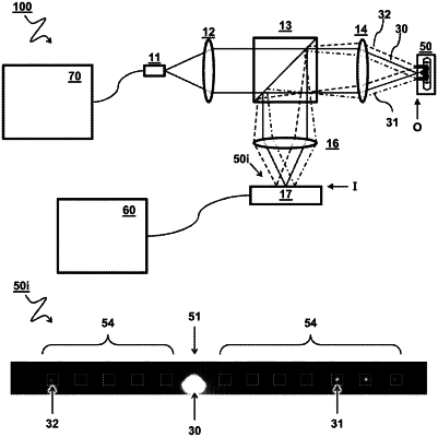
1. A method of interrogating an optical chip, the method comprising
illuminating the optical chip with input light;
using a detector to measure a spatially resolved image in which output light from the optical chip is imaged;
aligning a position of the input light on the optical chip based on a position of the output light and/or a reflection of the input light in the spatially resolved image; and
using the same detector to measure a spectral response of the optical chip based on an intensity of the output light in the spatially resolved image;
wherein the output light is emitted from a chip surface of the optical chip, and the input light is reflected from the chip surface, wherein the input and output light from the chip surface is projected by an imaging system onto a detector, wherein the imaging system is disposed in an optical path between the optical chip and the detector, wherein the optical chip is disposed in an object plane of the imaging system and the detector is disposed in an imaging plane of the imaging system.
|