| CPC G02B 1/12 (2013.01) [C23C 14/24 (2013.01); C23C 16/0245 (2013.01); G02B 1/113 (2013.01); G02B 1/118 (2013.01); B82Y 20/00 (2013.01); B82Y 30/00 (2013.01); B82Y 40/00 (2013.01)] | 17 Claims |
|
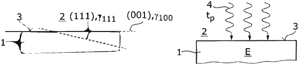
1. A method for forming nanostructures on a surface of a crystalline substrate for transmission of radiation in the far-ultraviolet/vacuum-ultraviolet (FUV/VUV) wavelength range, comprising:
providing a surface, which surface is not oriented along a lattice plane having a minimum surface energy, on the substrate or on a layer formed from a fluoridic crystal applied to the substrate by a coating method, and
introducing an energy input into the surface for rearranging the surface to form the nanostructures, wherein the energy input is generated by directly irradiating the surface with electromagnetic radiation.
|