| CPC G01R 31/2831 (2013.01) [H01L 21/6735 (2013.01); H01L 21/6773 (2013.01)] | 20 Claims |
|
1. A substrate analysis apparatus comprising:
an interlayer conveying module which is provided in a first region of the substrate analysis apparatus, and configured to transport a first Front Opening Unified Pod (FOUP) configured to store a plurality of wafers in a vertical direction;
an exchange module which is connected to the interlayer conveying module, and configured to transfer a wafer, from among the plurality of wafers, from the first FOUP to a second FOUP provided in a second region of the substrate analysis apparatus different from the first region;
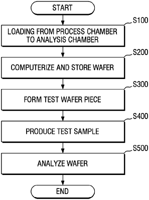
a pre-processing module which is provided in the second region, and configured to form a test wafer piece using the wafer inside the second FOUP;
an analysis module which is provided in the second region, and configured to analyze the test wafer piece; and
a transfer rail which is provided in the second region, and configured to transport the second FOUP containing the wafer and a tray containing the test wafer piece,
wherein the wafer comprises a first identifier indicating information corresponding to the wafer,
the test wafer piece comprises a second identifier indicating information generated by the pre-processing module which corresponds to the test wafer piece, and
the analysis module is configured to analyze the first identifier and the second identifier in connection with each other.
|