| CPC C30B 25/12 (2013.01) [C23C 16/4584 (2013.01); C23C 16/46 (2013.01); C30B 25/105 (2013.01); H01L 21/0262 (2013.01); H01L 21/68764 (2013.01); H01L 23/544 (2013.01); H01L 2223/54493 (2013.01)] | 10 Claims |

|
1. A device for depositing an epitaxial layer on a front side of a wafer having an orientation notch, comprising
a mechanism for holding and rotating a susceptor, the mechanism having a susceptor support shaft and susceptor support arms; and
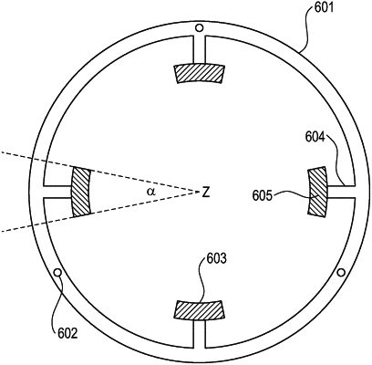
a ring positioned below the susceptor which is held by the susceptor support arms having a plurality of inwardly pointing projections at regularly spaced azimuthal positions corresponding to crystal orientation directions on the front side of the wafer which exhibit a higher epitaxial growth rate than other crystal orientation directions;
wherein the susceptor comprises a susceptor ring having a resting face for resting the wafer in an edge region of a back side of the wafer on the susceptor ring, a stepped outer boundary adjacent to the resting face, and a radially inward projection of the stepped outer boundary sized to fit within the orientation notch of the wafer, and wherein
the resting face has an inwardly pointing projection adjacent to the resting face at the same azimuthal position as the radially inward projection of the stepped outer boundary, and which extends below the orientation notch of the wafer.
|