US 11,981,991 B2
Sputter trap having a thin high purity coating layer and method of making the same
Jaeyeon Kim, Liberty Lake, WA (US); Patrick Underwood, Charlotte, NC (US); Susan D. Strothers, Mead, WA (US); Shih-Yao Lin, Hsinchu (TW); Michael D. Payton, Rockford, WA (US); and Scott R. Sayles, Mead, WA (US)
Assigned to Honeywell International Inc., Charlotte, NC (US)
Filed by Honeywell International Inc., Charlotte, NC (US)
Filed on Jan. 9, 2023, as Appl. No. 18/094,757.
Application 18/094,757 is a continuation of application No. 16/531,882, filed on Aug. 5, 2019, granted, now 11,584,985.
Claims priority of provisional application 62/717,994, filed on Aug. 13, 2018.
Prior Publication US 2023/0143320 A1, May 11, 2023
This patent is subject to a terminal disclaimer.
Int. Cl. H01J 37/34 (2006.01); C23C 14/34 (2006.01); C23C 14/56 (2006.01)
CPC C23C 14/564 (2013.01) [C23C 14/3407 (2013.01); H01J 37/3435 (2013.01); H01J 37/3491 (2013.01)] 20 Claims
OG exemplary drawing
 
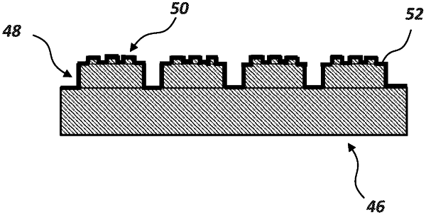
1. A sputtering chamber component comprising:
a front surface formed of an aluminum or copper alloy;
a back surface opposite the front surface;
a sputter trap formed on at least a portion of the front surface, the sputter trap having a surface roughness greater than the back surface of the sputtering chamber component; and
a coating of titanium particles formed on the sputter trap, the coating having a thickness from about 0.025 mm to about 2.54 mm (0.001 inches to about 0.1 inches) and is at least about 99.99% pure, wherein the titanium particles of the coating are substantially diffused and have plastic deformation.