| CPC B41J 2/04541 (2013.01) [B41J 2/04536 (2013.01); B41J 2/04586 (2013.01); G11C 17/16 (2013.01); G11C 17/18 (2013.01)] | 18 Claims |
|
1. An element substrate, comprising:
a plurality of groups of print elements;
a plurality of groups of memory elements;
a plurality of stages of shift registers configured to input and hold a serial data signal;
a latch circuit configured to latch the serial data held by the shift registers;
a decoder circuit configured to input an output of the latch circuit and output a selection signal for selecting a block of the print elements or the memory elements; and
a mask circuit configured to mask the output of the selection signal for selecting the block of the memory elements from the decoder circuit in accordance with an input bit data signal, wherein
the block of the print elements or the memory elements includes a plurality of print elements or memory elements in which one element is selected in each of the plurality of groups, and
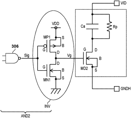
the memory elements are one time programmable memory elements, each of which stationary holds information and functions as a memory that can be programmed only once.
|