| CPC B41J 2/04541 (2013.01) [B41J 2/0455 (2013.01); B41J 2/04581 (2013.01); B41J 29/377 (2013.01)] | 10 Claims |
|
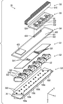
1. A head unit having a first driving element group driven by a first driving signal and a second driving element group driven by a second driving signal and discharging a liquid in response to drive of the first driving element group and the second driving element group, comprising:
a substrate that propagates the first driving signal and the second driving signal;
a first driving circuit disposed on the substrate and outputting the first driving signal;
a second driving circuit disposed on the substrate and outputting the second driving signal;
a heat sink fixed to the substrate; and
a plurality of heat conductive elastic bodies positioned between the substrate and the heat sink, wherein
the first driving circuit includes a first integrated circuit that outputs a first gate signal based on a first reference driving signal that is a reference of the first driving signal, a first amplifier circuit including a first transistor driven by the first gate signal, and a first smoothing circuit that smoothes output from the first amplifier circuit and outputs the first driving signal,
the second driving circuit includes a second integrated circuit that outputs a second gate signal based on a second reference driving signal that is a reference of the second driving signal, a second amplifier circuit having a second transistor driven by the second gate signal, and a second smoothing circuit that smoothes output from the second amplifier circuit and outputs the second driving signal,
a first heat conductive elastic body among the plurality of heat conductive elastic bodies is positioned between the heat sink and the first integrated circuit, and is in contact with the heat sink and the first integrated circuit,
a second heat conductive elastic body among the plurality of heat conductive elastic bodies is positioned between the heat sink and the first transistor, and is in contact with the heat sink and the first transistor,
a third heat conductive elastic body among the plurality of heat conductive elastic bodies is positioned between the heat sink and the second integrated circuit, and is in contact with the heat sink and the second integrated circuit,
a fourth heat conductive elastic body among the plurality of heat conductive elastic bodies is positioned between the heat sink and the second transistor, and is in contact with the heat sink and the second transistor, and
the heat sink has a first recess portion positioned between a first contact portion which is in contact with the first heat conductive elastic body and a second contact portion which is in contact with the second heat conductive elastic body, and a second recess portion positioned between a third contact portion which is in contact with the third heat conductive elastic body and a fourth contact portion which is in contact with the fourth heat conductive elastic body.
|