| CPC H01L 29/0673 (2013.01) [H01L 27/088 (2013.01); H01L 21/02603 (2013.01); H01L 21/823412 (2013.01); H01L 21/823431 (2013.01); H01L 21/823807 (2013.01); H01L 21/823821 (2013.01); H01L 21/84 (2013.01); H01L 21/845 (2013.01); H01L 29/0665 (2013.01); H01L 29/401 (2013.01); H01L 29/42376 (2013.01); H01L 29/42392 (2013.01); H01L 29/4983 (2013.01); H01L 29/66439 (2013.01); H01L 29/66545 (2013.01); H01L 29/775 (2013.01); H01L 29/78651 (2013.01); H01L 29/78696 (2013.01)] | 41 Claims |

|
[ 20. A method of forming nano-sheet devices, the method comprising:
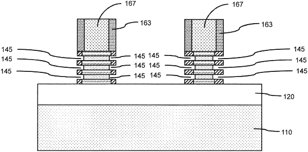
providing at least two dummy gate structures, each of the dummy gate structures (i) disposed on a cut-stack comprising alternating sacrificial release layers and nano-sheet channel layers and (ii) comprising opposing side spacers, each side spacer having opposing inside and outside surfaces;
forming first lateral indentations of a first depth in a first plurality of sacrificial release layers of a first cut-stack;
forming second lateral indentations of a second depth in a second plurality of sacrificial release layers of a second cut-stack, wherein the second depth is greater than the first depth; and
filling the first lateral indentations in the first cut-stack and the second lateral indentations in the second cut-stack with a dielectric material. ]
|