| CPC H10K 59/131 (2023.02) [H10K 59/122 (2023.02); H10K 59/40 (2023.02); H10K 77/111 (2023.02); G06F 3/0412 (2013.01)] | 16 Claims |

|
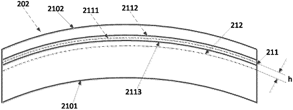
1. A flexible display panel, comprising a display area and a non-display area, wherein the non-display area comprises a bending sub-area and a binding sub-area, and the bending sub-area is configured to bend the binding sub-area to a side away from the display area;
the display area comprises a driving circuit layer arranged on a substrate, the driving circuit layer comprises a source/drain electrode layer, a planarization layer arranged at a side, far away from the substrate, of the source/drain electrode layer, a pixel defining layer arranged at a side, far away from the substrate, of the planarization layer and a touch wiring layer arranged at a side, far away from the substrate, of the pixel defining layer, the bending sub-area comprises a first organic layer, a second organic layer and a metal wiring layer between the first organic layer and the second organic layer arranged on the substrate, the touch wiring layer is electrically connected to the metal wiring layer, and an orthographic projection of the touch wiring layer on a plane of the substrate is not located in the bending sub-area;
in response to the bending sub-area being in a bending state, a vertical distance from a bending neutral layer of the bending sub-area to the metal wiring layer is smaller than a preset distance.
|