| CPC H10K 59/131 (2023.02) [H10K 59/351 (2023.02); H10K 59/353 (2023.02)] | 17 Claims |

|
1. A display substrate, comprising:
a base substrate;
a pixel defining layer, disposed on the base substrate and including a plurality of openings; and
at least one photo spacer, disposed on a side of the pixel defining layer away from the base substrate, wherein
a distance from any point at a bottom of the at least one photo spacer contacting the pixel defining layer to an upper edge of a side wall of the plurality of openings is greater than or equal to 5 μm,
wherein the display substrate further comprises:
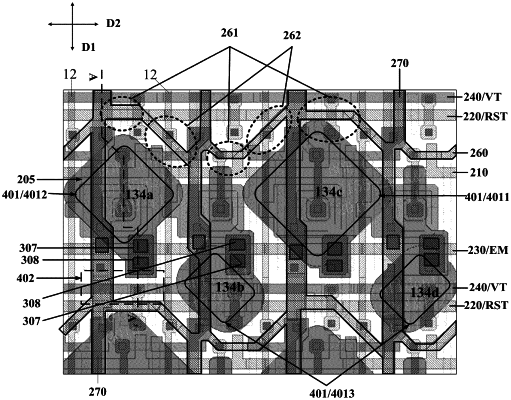
a pixel circuit structure, disposed between the base substrate and the pixel defining layer and including a first signal line and a second signal line which are parallel to each other, wherein
a first orthographic projection of the at least one photo spacer on the base substrate is located between a second orthographic projection of the first signal line on the base substrate and a third orthographic projection of the second signal line on the base substrate.
|