| CPC H10K 59/131 (2023.02) [H10K 50/844 (2023.02); H10K 71/00 (2023.02); H10K 59/1201 (2023.02); H10K 59/88 (2023.02)] | 20 Claims |

|
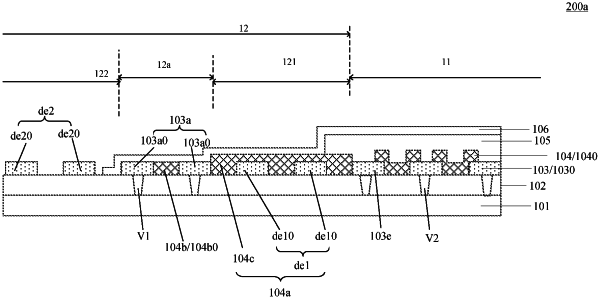
1. A display substrate, comprising:
a base substrate;
a first insulation layer, located on the base substrate;
a first electrode pattern, located in a display region of the display substrate, the first electrode pattern comprising a plurality of first electrodes spaced apart from each other, and each of the plurality of first electrodes being configured to receive a pixel driving signal;
a connecting electrode pattern, located in a peripheral region of the display substrate, the connecting electrode pattern surrounding the first electrode pattern;
a second electrode, located in the display region and the peripheral region and connected with the connecting electrode pattern, the second electrode and the first electrode pattern being spaced apart from each other, and the second electrode being configured to receive a first power signal;
a light-emitting functional layer, located between the first electrode pattern and the second electrode; and
a first filling layer, located between the connecting electrode pattern and the first electrode pattern,
wherein the first filling layer and the light-emitting functional layer are different layers; and
the first electrode pattern and the connecting electrode pattern are located at a side of the first insulation layer away from the base substrate, and are in contact with the first insulation layer, respectively; a portion of the first insulation layer that is located between the first electrode pattern and the connecting electrode pattern has a groove, and the first filling layer is at least partially located in the groove.
|