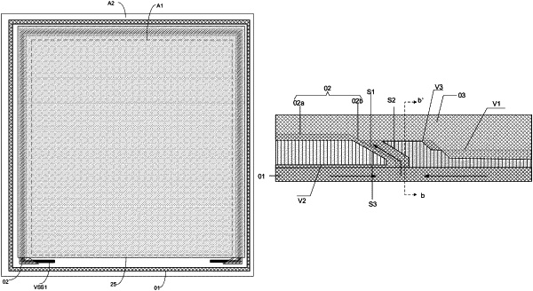
| CPC H10K 59/122 (2023.02) [H10K 50/844 (2023.02)] | 16 Claims |

|
1. A display panel, comprising a base substrate, wherein the base substrate is provided with a display area and a bezel area surrounding the display area; the bezel area comprises a first dam surrounding the display area;
the display area comprises an anode layer, a light-emitting layer and a cathode layer arranged on a side of the base substrate in sequence in a laminated mode;
a first metal layer, a first planarization layer, an anode lap joint layer, a pixel defining layer and the cathode layer arranged on the side of the base substrate in sequence in a laminated mode are disposed between the first dam and the display area;
the first metal layer at least comprises a first supply voltage wire;
the anode lap joint layer and the anode layer are arranged on a same layer;
the cathode layer is electrically connected with the first supply voltage wire through the anode lap joint layer;
the anode lap joint layer comprises a main body portion and sharp angle portions located at two ends of the main body portion; the sharp angle portion at least comprises a first side edge close to the display area; the first side edge of the sharp angle portion close to the display area is an oblique edge, and an included angle between the oblique edge and a border of the display area adjacent to the oblique edge is larger than 0° but smaller than or equal to 30°;
the pixel defining layer wraps a border of the anode lap joint layer and is provided with a first groove, the first groove extends from one sharp angle portion of the anode lap joint layer to the other sharp angle portion of the anode lap joint layer, is located at a side of the sharp angle portion far away from the main body portion and is formed at a side of the sharp angle portion close to the display area, an edge of the first groove adjacent to the first side edge of the sharp angle portion is a second side edge, and an outline of the second side edge is consistent with an outline of the first side edge; and
the first planarization layer is provided with a second groove, and an orthographic projection of the second side edge on the base substrate is located in an orthographic projection of the second groove on the base substrate.
|