| CPC H10K 50/865 (2023.02) [G06F 3/0412 (2013.01); H10K 50/844 (2023.02); H10K 50/854 (2023.02); H10K 59/38 (2023.02); H10K 59/40 (2023.02)] | 19 Claims |

|
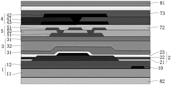
1. An organic light-emitting diode (OLED) display panel, comprising:
a drive backplane; and
an OLED device, an encapsulation structure and a color resistor structure which are arranged on the drive backplane;
wherein the encapsulation structure and the color resistor structure are arranged on a side, facing away from the drive backplane, of the OLED device;
the color resistor structure comprises a chromatic color resistor layer, a first black matrix (BM) and a second BM;
the first BM is arranged on a side, facing away from the drive backplane, of the chromatic color resistor layer, and the second BM is arranged on a side, facing the drive backplane, of the chromatic color resistor layer;
the side, facing away from the drive backplane, of the OLED device is provided with at least one scattering layer; and
the at least one scattering layer comprises an organic material film and scattering particles arranged in the organic material film.
|