| CPC H10K 50/856 (2023.02) [H10K 59/122 (2023.02); H10K 71/00 (2023.02); H10K 2102/3026 (2023.02)] | 15 Claims |

|
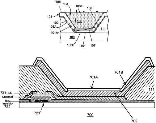
1. An light-emitting diode (LED) device to provide a pixel of a display, the device comprising:
a substrate;
a well structure on the substrate, wherein the well structure includes a recess with side walls and a floor;
a lower metal layer covering the floor and side-walls of the well structure;
an upper conductive layer on the lower metal layer covering the floor of the well structure and contacting the lower metal layer, the upper conductive layer having outer edges at about an intersection of the side walls and the floor;
a dielectric layer formed of an oxide of the lower metal layer covering the side walls of the well structure without covering the upper conductive layer;
a stack of LED layers covering at least the floor of the well structure, the upper conductive layer providing a lower electrode for the stack of LED layers; and
a light extraction layer (LEL) in the well structure over the stack of LED layers and the dielectric layer.
|