| CPC H10K 50/8426 (2023.02) [H10K 59/131 (2023.02); H10K 71/00 (2023.02); H01L 25/18 (2013.01); H10K 59/1201 (2023.02)] | 20 Claims |

|
1. A display substrate, comprising a display area and a non-display area surrounding the display area, wherein:
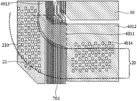
the non-display area comprises a sealant region surrounding the display area; the sealant region comprises: a corner sealant region, a lead-in sealant region, and a first sealant region that are on a first side of the display area, and the first sealant region is located between the corner sealant region and the lead-in sealant region; the corner sealant region is provided with an encapsulation base layer; the non-display area is provided with a second power line, a gate drive circuit, and a plurality of first signal lines configured to provide a signal to the gate drive circuit;
the second power line comprises a power line corner portion and a first power line portion, the first power line portion overlaps the first sealant region, and the first power line portion extends in a first direction; and
a target portion of each of the first signal lines is at least located in the corner sealant region, and the target portion extends in a second direction; the first direction intersects the second direction; an orthographic projection of the target portion onto a base substrate of the display substrate is located between an orthographic projection of the encapsulation base layer onto the base substrate and an orthographic projection of the first power line portion onto the base substrate.
|