| CPC H10B 10/12 (2023.02) [H01L 21/0274 (2013.01); H01L 21/31144 (2013.01); H01L 21/76802 (2013.01); H01L 21/76877 (2013.01); H01L 27/0207 (2013.01); H10B 10/125 (2023.02)] | 18 Claims |

|
1. A method of fabricating an integrated circuit having an SRAM, comprising:
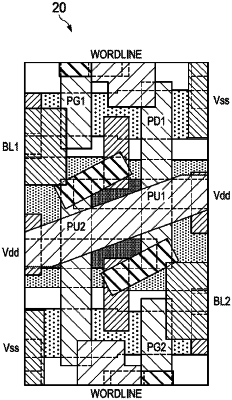
forming a gate layer having a first gate structure with a long dimension extending in a first direction, the long dimension being a width or a length from a top down view of the SRAM;
forming a contact layer having a first contact with a first portion with a long dimension extending in the first direction, the long dimension being a width or a length from the top down view and a second portion with a long dimension extending in a second direction at a diagonal from the first direction, the long dimension being a width or a length from the top down view;
forming a power (Vdd) routing in a metal-1 layer, a portion of the power routing extending over the first gate structure and having a long dimension that extends in a third direction at a diagonal from the first direction, the long dimension being a width or a length from the top down view, wherein the portion of the power routing is defined with a first metal-1 mask and the metal-1 layer includes one or more portions defined with a second metal-1 mask different than the first metal-1 mask; and
a first bit line routing and a second bit line routing in a metal-2 layer.
|